VLSI LabSchool of Computer & Systems Sciences, JNU, New Delhi
Jawaharlal Nehru University, New Delhi

VLSI Lab

Research in VLSI design, nano electronics and low-power circuits for next-generation computing.

Meet our faculty →
VLSI

About

Very-large-scale integration (VLSI) creates integrated circuits by combining millions of transistors on a single chip. Designing VLSI systems with next-generation technologies requires collaboration across system architecture, logic and circuit design, fabrication, packaging and testing.

The VLSI Lab at the School of Computer & Systems Sciences, Jawaharlal Nehru University, works on nanoscale devices, low-power circuits, mixed-signal design, microsystems, EDA tools and AI in VLSI design. Its scholars and alumni now work at research institutes and universities in India and abroad.

ASDr. Asutosh Srivastava
Faculty

Dr. Asutosh Srivastava

Assistant Professor · Chief Investigator, Chip 2 Startup (C2S) programme at JNU
VLSI / Nano-electronics, EDA tools, AI in VLSI design

Full profile

Collaboration

🌏

Prof. Masahiro Fujita

VLSI Design and Education Center (VDEC), University of Tokyo, Japan

🌎

Prof. Manoj Sachdev

Department of Electrical and Computer Engineering, University of Waterloo, Canada

🏛️

Inter-University Accelerator Centre (IUAC)

New Delhi, India

Research Area


🔌

VLSI / Nano-electronics & EDA Tools in VLSI Design

Nanoscale devices, high-k dielectrics and next-generation lateral bipolar transistors for mixed-signal circuits, designed with industry-standard EDA flows using licensed Cadence and Synopsys tools through the C2S programme.

🤖

AI in VLSI Design

Applying machine learning to design, optimisation and verification of integrated circuits.

✅

VLSI Verification

Methods to verify chip designs at system, logic and circuit levels.

🧪

VLSI Technology

Investigation of next-generation fabrication techniques for etching and deposition of thin films, and lithography, in MIM, MOS and MOSFET devices with advanced feature sizes.

🧠

Neuromorphic Computing / AI Hardware

Brain-inspired, ultra-low-power AI hardware for intelligent systems and IoT.

📡

Sensors and IoT Hardware

Low-power sensors and ultra-low-power sensors circuits and systems for IoT applications.

Facilities


The lab provides EDA VLSI design tools such as Cadence, Siemens and Synopsys. Through the Chip to Startup (C2S) programme, JNU UG, M.Tech and Ph.D. students get access to licensed tools from Cadence and Synopsys.

🧩

Cadence

EDA VLSI design tools.

💠

Siemens

EDA VLSI design tools.

🔷

Synopsys

EDA VLSI design tools.

Research Profile

ASDr. Asutosh Srivastava
Assistant Professor

Dr. Asutosh Srivastava

School of Computer & Systems Sciences, Jawaharlal Nehru University, New Delhi · Room No. 12
asutosh@mail.jnu.ac.in · ashudel07@gmail.com · 011-26708785

Qualifications

  • M.E., Electrical and Electronics Engineering, Nanyang Technological University, Singapore
  • Ph.D., Electronics and Telecommunication Engineering, Jadavpur University, Kolkata

Areas of Interest / Specialization

VLSI / Nano-electronicsEDA tools in VLSI designAI in VLSI designVLSI verificationVLSI TechnologyNeuromorphic computing / AI hardware

Chip to Startup (C2S) Programme

Chief Investigator at JNU for the Chip to Startup (C2S) programme under MeitY, Government of India. Through C2S, JNU UG, M.Tech and Ph.D. students get access to licensed VLSI design tools such as Cadence and Synopsys.

Experience

Assistant Professor, School of Computer & Systems Sciences, JNUFeb 2014 – present
Associate Professor, Dept. of Electronics & Communication Engineering, PDPM-IIITDM Jabalpur2012 – 2014
Assistant Professor, Dept. of Electronics & Communication Engineering, PDPM-IIITDM Jabalpur2009 – 2012
Lecturer, Electrical & Electronics Engineering Dept., BITS PilaniDec 2005 – 2009

Latest Publications with Students

Journal Papers

  • S. Suman, A. Sarkar, A. Srivastava, “Study of extended channel double gate TFET with injection of Ge quantum dot for extremely low power AI chip applications”, Micro and Nanostructures, 208849, 2026.
  • S. Suman, A. Srivastava, “Sensitivity analysis of DG-TFET based biosensor with injection of quantum dot”, Physica Scripta, 101(30), 305917, 2026.
  • S. Suman, A. Srivastava, “Study of quantum dot injected inside double gate IT-TFET for digital and analog chip applications”, Physica Scripta, 100(9), 095947, 2025.
  • S. Suman, A. Srivastava, A. Sarkar, “Comparative Study of Double Gate Inverted-T Shaped, TFET for Extremely Low Power Logic and Analog Circuit in AI Chips”, Silicon, 17(15), 3585–3600, 2025.
  • Jitendra Kumar, Yukio Miyasaka, Asutosh Srivastava, Masahiro Fujita, “Formal Verification of Integer Multiplier Circuits Using Binary Decision Diagrams”, IEEE Trans. on Computer-Aided Design of Integrated Circuits and Systems, 42(4): 1365–1378, 2023.

Conference Papers

  • S. Suman, A. Srivastava, “Study of dual extended sources double gate TFET for extremely low power applications”, 2025 IEEE 20th Nanotechnology Materials and Devices Conference (NMDC), pp. 17–21, 2025.
  • D. K. Panday, S. Suman, S. Khan, A. Srivastva, “Fabrication and characterization of alumina based resistive RAM for space applications”, 2024 IEEE 24th International Conference on Nanotechnology (NANO), pp. 253–257, 2024.
  • S. Suman, R. Kumar, A. Srivastva, “Inverted T-Shaped Tunnel Field-Effect Transistors for Extremely Low Power Chip Applications”, 2024 IEEE 24th International Conference on Nanotechnology (NANO), pp. 219–223, 2024.
  • Jitendra Kumar, Asutosh Srivastava, Masahiro Fujita, “Formal Analysis of Integer Multipliers by building Binary Decision Diagram of Adder Trees”, ISQED 2022, pp. 58–63.
  • Jitendra Kumar, Asutosh Srivastava, “Dynamic Variable Ordering during Algebraic Backward Rewriting for Formal Verification of Multipliers”, VLSID 2022, pp. 28–32.

Source: Google Scholar and dblp.org. This list may be incomplete.

Best Peer-Reviewed Publications

  • A. Srivastava et al., “Study of La-Incorporated HfO2 MIM Structure Fabricated Using PLD System for Analog/Mixed Signal Applications”, IEEE Transactions on Nanotechnology, Vol. 14(4), 2015, pp. 612–618.
  • A. Srivastava, P. Sarkar, C. K. Sarkar, “Study in variation of Gate Dielectric permittivity with different EOT on channel engineered Deep Sub-micrometer n-MOSFET Device for Mixed Signal Applications”, Microelectronics Reliability, Vol. 49(4), 2009, pp. 365–370.
  • D. Zade, S. Sato, K. Kakushima, A. Srivastava, P. Ahmet, K. Tsutsui, A. Nishiyama, N. Sugii, K. Natori, T. Hattori, C. K. Sarkar, H. Iwai, “Effects of La2O3 incorporation in HfO2 gated nMOSFETs on low-frequency noise”, Microelectronics Reliability, 51(4), 2011, pp. 746–750.

Book Chapter

Article in Section II (Nano-CMOS Technology), in J. E. Morris & K. Iniewski (eds.), Nanoelectronic Device Applications Handbook, CRC Press (Taylor & Francis), ISBN 9781466565234.

International Collaboration / Consultancy

  • Prof. Masahiro Fujita, VLSI Design and Education Center, University of Tokyo, Japan
  • Prof. Manoj Sachdev, Dept. of Electrical and Computer Engineering, University of Waterloo, Canada

National Collaboration

  • Inter-University Accelerator Centre (IUAC), New Delhi

Awards & Honours (international programmes)

Nanyang Technological University, SingaporeCERN, Switzerland / FranceDST-JSPS, Tokyo Institute of Technology, JapanJenesys, VLSI Design Center, University of TokyoIUSSTF, Electrical Engineering, Yale University, USA

Members


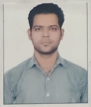
Click a photo to open the full profile and publications.

Mr. Dharmendra Kumar Panday
Ph.D. Scholar

Mr. Dharmendra Kumar Panday

Current: Pursuing a Ph.D. in VLSI & Microsystems, SC&SS, JNU, New Delhi – 110067

Ph.D.: VLSI & Microsystems (pursuing), SC&SS, JNU, New Delhi – 110067

M.Tech thesis: VLSI Lab, SC&SS, JNU, New Delhi – 110067

Email: dk290558@gmail.com

Phone: +91 7493004015
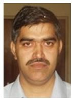
Dr. Kundan Singh
Ph.D. Alumnus

Dr. Kundan Singh

Current: Engineer-G, Inter-University Accelerator Centre (IUAC), GOI, New Delhi – 110067

Ph.D.: VLSI / Semiconductor, VLSI Lab, SC&SS, JNU, New Delhi – 110067

M.Tech: NIT Kurukshetra, Haryana
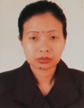
Dr. Lourembam Beloni Devi
Ph.D. Alumna

Dr. Lourembam Beloni Devi

Current: Assistant Professor, NIELIT, Imphal

Ph.D.: VLSI / Semiconductor, VLSI Lab, SC&SS, JNU, New Delhi – 110067

M.Tech: CSIR-CEERI, Pilani
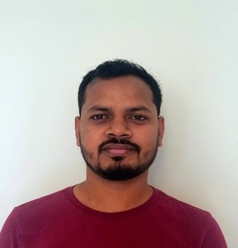
Dr. Jitendra Kumar
Ph.D. & M.Tech Alumnus

Dr. Jitendra Kumar

Current: Member of Technical Staff, AMD, Bangalore; Formal Verification Lead, Intel, Bangalore

Ph.D.: VLSI / Semiconductor, VLSI Lab, SC&SS, JNU, New Delhi – 110067

M.Tech: VLSI Lab, SC&SS, JNU, New Delhi – 110067
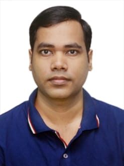
Dr. Rakesh Kumar
Ph.D. Alumnus

Dr. Rakesh Kumar

Current: Assistant Professor, University of Delhi

Ph.D.: VLSI / Semiconductor, VLSI Lab, SC&SS, JNU, New Delhi – 110067
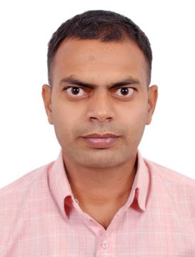
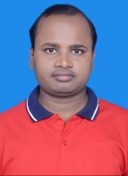
Mr. Pradeep Singh
M.Tech Alumnus

Mr. Pradeep Singh

Current: Pursuing Ph.D., Institute of Communications Engineering, National Sun Yat-sen University, Kaohsiung, Taiwan

M.Tech thesis: VLSI Lab, SC&SS, JNU, New Delhi – 110067

BK
M.Tech Student

Mr. Bikash Kundu

M.Tech: VLSI Lab, SC&SS, JNU, New Delhi – 110067

Events

Contact


VLSI Lab, School of Computer & Systems Sciences

Jawaharlal Nehru University, New Mehrauli Road, New Delhi – 110067

Dr. Asutosh Srivastava (Room No. 12): asutosh@mail.jnu.ac.in · 011-26708785